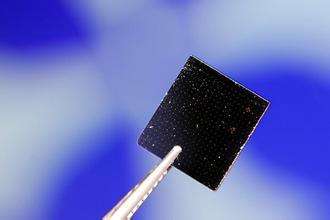
[China Instrument Network Instrument R&D] The Korea Science and Technology Research Institute released the news that the joint Yonsei University's development of a two-dimensional tungsten selenide nano single chip and a one-dimensional zinc oxide semiconductor nanowire hybrid space double layer structure, development Photodiode devices that can sense from ultraviolet to near-infrared light.
(Image from the Internet, invaded)
The study was published in the Advanced Academic Materials, an international academic magazine.
Low-dimensional nano-semiconductor devices have broad application prospects in the next-generation semiconductors and are key research and development fields. The two-dimensional element used by the research group has the characteristics of strong light-response performance and high hole mobility and is a P-type semiconductor element.
One-dimensional zinc oxide nanowires are one of the best one-dimensional nano-semiconductors currently available, have high electron mobility characteristics, and are expected to be applied to high-performance electronic component N-type semiconductor devices. After one-dimensional two-dimensional mixing, a hybrid dimensional space double-layer structure (PN type) was formed and a photodiode element was developed.
The research group stated that the study successfully achieved two-dimensional images and is expected to be widely used in next-generation image sensor components.
(Original Title: Korea Develops Next-Generation Nano Semiconductor Image Sensors)